






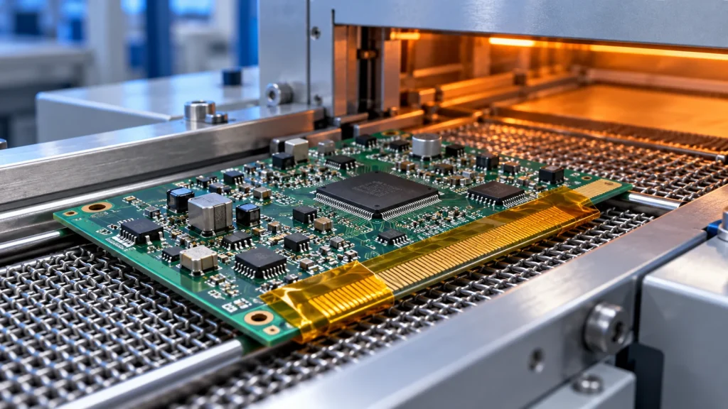
Temporary masking succeeds when it protects the intended feature, survives the complete assembly process, and comes off without creating a new defect. A film that looks intact after heating can still fail through adhesive transfer, edge movement, trapped flux, or damage during removal.
For engineers selecting high-temperature masking materials, the useful unit of qualification is the complete masking construction on the actual assembly under a defined process window. The backing polymer alone is not a solder-process specification.
This guide covers temporary tapes, die-cut masks, peelable compounds and reusable shielding approaches. It does not cover permanent photoimageable PCB solder mask. Material comparisons below are general engineering guidance; they are not performance specifications for any HighTemp Material grade.
1. Start with the exposure: reflow and wave soldering are different problems
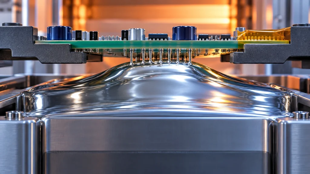
Reflow: the full time–temperature history matters
In convection reflow, the assembly experiences preheating, a process-dependent soak or ramp, solder reflow and cooling. The relevant temperature is measured at the assembly and masking location, rather than inferred from an oven-zone setpoint.
Document peak temperature, dwell at elevated temperature, heating and cooling rates, atmosphere, and total passes. Double-sided assembly and later rework can add exposure. A short successful laboratory heat exposure does not establish suitability for repeated production cycles.
A thin masking film usually provides a barrier to contamination or unwanted contact; it is not a reliable thermal shield for a temperature-sensitive component. If the protected component must remain cooler, evaluate a purpose-designed shield, assembly sequence change or process adjustment, and measure the resulting component temperature.
Wave and selective soldering: contact and edge integrity matter
Wave soldering adds flux, preheat and local molten-solder exposure. Selective soldering can impose concentrated exposure around a nozzle path. Solder-pot temperature does not describe either the full PCB thermal history or the temperature at every masking interface.
Establish which side faces solder, whether the mask is directly contacted, contact duration, wave orientation, repeated passes and pallet support. A material approved for hot-air exposure must not automatically be approved for immersion or direct solder contact.
| Process condition | Main masking challenge | Information needed before selection |
|---|---|---|
| Convection reflow | Dimensional stability, adhesive aging, repeated heating | Measured profile at relevant sites, atmosphere, passes |
| Wave soldering | Edge sealing, solder ingress, flux compatibility | Contact side and time, flux, preheat, pallet geometry |
| Selective soldering | Local heat and nozzle clearance | Nozzle path, contact envelope, nearby features |
| Rework | Concentrated heat and accumulated damage | Tool, local profile, prior thermal history, removal plan |
Engineering decision: classify hot-air exposure and direct molten-solder contact separately in the RFQ and qualification plan.
2. Understand the complete masking construction
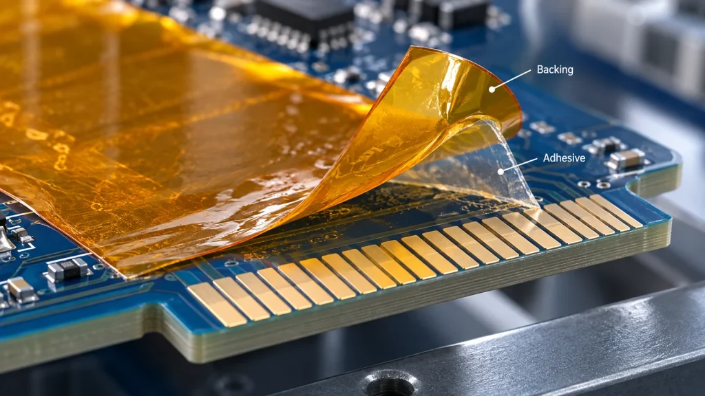
Backing, adhesive and liner have different jobs
The backing provides coverage and handling strength. Its behavior during the process includes shrinkage, curling, stiffness changes and tear resistance. The adhesive must wet the board sufficiently, hold the boundary during processing and release under the agreed removal conditions.
A release liner supports storage, converting and application. It normally leaves the assembly before processing. Do not assume that liner chemistry, release transfer or liner particles are irrelevant to a sensitive surface. If the liner remains during any operation, qualify that unusual construction explicitly.
Specify backing thickness, adhesive coat thickness and total thickness separately where available. Total tape thickness cannot be substituted for backing thickness in a drawing.
Silicone and acrylic are families, not approval categories
Silicone adhesives are used in many solder-masking tapes, but the word “silicone” does not establish clean removal, low contamination or a particular process limit. Acrylic constructions can be useful where their exact grade meets the exposure and surface requirements. Neither chemistry should be selected from its name alone.
For silicone-restricted assemblies, obtain a construction-specific declaration covering the adhesive, liner and other relevant processing materials. Visually clean removal does not prove absence of transferable species. Where later coating, bonding or contact performance is sensitive, test those downstream operations.
Initial tack and room-temperature peel strength also do not establish hot holding power or post-process removability. Excessively aggressive adhesion may damage a weak coating or fine feature; insufficient adhesion can allow edge lift.
3. Compare masking solutions by function
| Solution | Reason to evaluate it | Principal limitation | Evidence to request |
|---|---|---|---|
| Polyimide film with qualified silicone adhesive | Candidate for demanding solder-process exposure and thin conformable masks | Adhesive transfer, removal force and downstream compatibility remain grade-specific | Complete-construction TDS, profile qualification, residue and removal results |
| Polyimide with qualified non-silicone adhesive | Candidate when silicone restrictions drive selection | A non-silicone label does not establish heat resistance or ionic cleanliness | Chemistry declaration, thermal-aging and functional compatibility data |
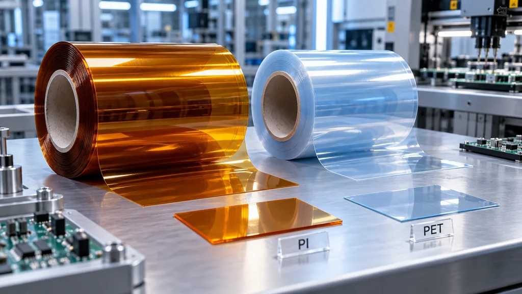
| PET masking construction | Candidate for selected protection or less demanding thermal conditions | Shrinkage and adhesive behavior can exclude it from the required solder profile | Grade identification, measured shrinkage, actual-profile results |
| Specialty fluoropolymer or composite construction | Candidate where release or chemical resistance motivates investigation | Backing suitability does not establish adhesive performance or edge sealing; availability varies | Application-specific construction and contact compatibility data |
| Peelable masking compound | Candidate for selected irregular regions or openings | Cure, removal access, trapped material and process compatibility require control | Current TDS/SDS, cure instructions, approved process and removal evidence |
| Reusable solder pallet or fitted shield | Candidate for repeatable large areas or selective exposure | Fixture clearances, wear and changed heat flow must be managed | Tooling drawing, profile validation, inspection and maintenance plan |
This table is a shortlist, not a ranking. A conformable tape and a reusable pallet can be complementary when their interaction is validated.
Why polyimide is a starting point, not a universal guarantee
Commercial polyimide solder-masking tapes demonstrate why backing and adhesive must be specified together. As one external product example, 3M’s retrieved July 2026 technical data for Tape 5413 identifies a polyimide backing with silicone adhesive and lists PCB solder masking applications up to 260°C. The document describes its data as typical rather than specification limits. This example is not an HTM specification, an equivalence claim, or approval of an arbitrary exposure duration. [1]
For candidate constructions, discuss the application through HighTemp Material’s polyimide tape product page. Confirm the actual offered grade and documentation before selection. Polyimide is the generic polymer name; Kapton® is a trademark and should only identify an authenticated branded material.
Where PET needs particular caution
A PET tape sold for another heated industrial process is not automatically suitable for solder reflow. Thermal shrinkage, directionality, prior heat stabilization and adhesive formulation all affect the outcome. A film may remain in one piece while moving enough to uncover a contact edge.
HighTemp Material’s PET masking film for SMT reflow page explicitly calls for qualification of the full construction under the customer’s actual profile. Treat PET as a candidate requiring evidence, rather than a cost-equivalent replacement for polyimide.
Where no suitable grade data exist, screen representative samples before developing a production quotation. Do not use a generic resin temperature, melting point or flame rating as proof of solder-masking suitability.
4. Design the mask around the feature and removal operation
Define coverage and keep-out boundaries
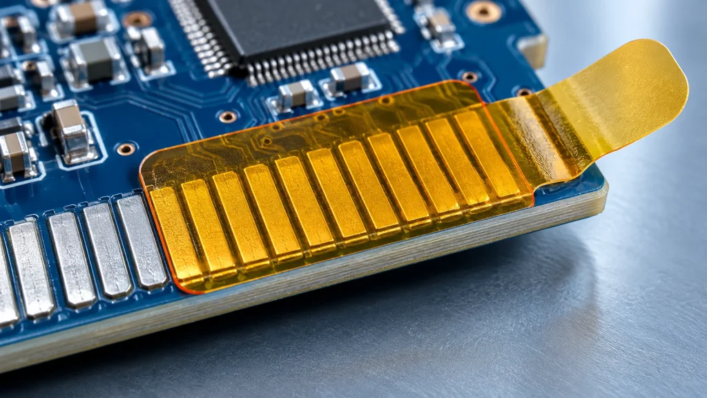
A mask drawing should identify the protected region, permissible overlap, exposed solderable regions and registration datum. Include tolerances for the die-cut part, PCB feature location and placement method. The combined variation determines whether protection remains adequate in production.
For a contact edge, verify that all required contact surfaces are covered without leaving adhesive on a functional area after removal. For holes or slots, distinguish a surface cover from a plug: material that sags or enters an opening may become difficult to remove.
Do not specify a universal overlap distance. Determine it from feature geometry, material movement, placement variation and the solder-contact condition, then verify the result on representative parts.
Avoid stretching, bridging and inaccessible peel starts
Apply a mask without stretching the film. Stored strain can encourage edge withdrawal during heating. Seat the boundary using a controlled application method without crushing components or damaging the finish.
A mask bridging a step can leave a channel for flux or solder. Segment the mask or revise the geometry if it cannot seat consistently. Rounded corners and a deliberately positioned removal tab are useful design candidates, but the tab must not lift into the solder path, obstruct handling or contact nearby components.
Use the chosen removal direction in the drawing or work instruction. Avoid pulling across vulnerable components or unsupported flex sections. Removal temperature, peel rate and angle belong in the validated process, rather than being left to operator preference.
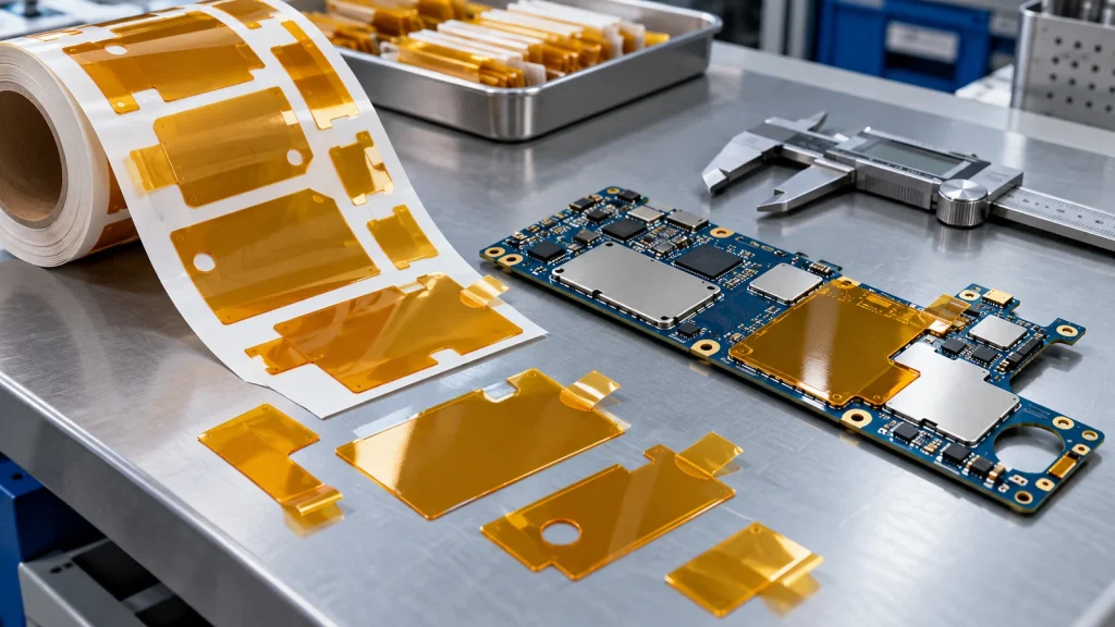
For repeated geometries, custom die cutting can be evaluated to improve presentation and placement consistency. Confirm tolerances, liner format, peel-tab design and inspection criteria for the actual material.
5. Typical industrial applications
Gold fingers and edge connectors
The objective is to prevent unwanted solder or process contamination while preserving contact function. Qualify both the protected boundary and the contact condition after removal. Visual appearance alone may not resolve a marginal contact-resistance issue.
Through-hole and selective soldering assemblies
Masks or pallets may protect nearby areas while leaving intended joints exposed. Check shadowing, flux accumulation, clearances and joint formation near the masking boundary. A wider mask is not automatically safer if it obstructs a joint.
Flexible circuits and delicate finishes
Conformability and removal force can dominate the decision. Support the substrate during application and removal, and inspect for finish lifting, pad damage, distortion and tearing. Do not infer behavior on flexible circuits from a steel peel test.
Battery-management, power-control and industrial electronics
For BMS boards, inverter control boards and related electronics, the relevant exposure is the PCB assembly process. This does not imply placing assembled battery cells or packs through a solder reflow oven. High-impedance sensing circuits, connectors and later coating steps may require additional residue or functional evaluation.
6. Failure risks and preventable selection errors
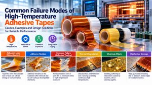
| Failure or mistake | Plausible mechanism | Prevention and verification |
|---|---|---|
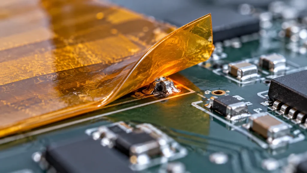
| Edge lift or boundary movement | Poor seating, stretched film, shrinkage, incompatible surface | Control application; measure boundaries before and after the full sequence |
| Solder or flux under the mask | Channels, wrinkles, steps or inadequate edge contact | Revise geometry and contact orientation; inspect the protected interface |
| Adhesive residue or staining | Heat aging, surface interaction or unsuitable removal condition | Compare constructions on actual finishes; inspect after realistic removal delays |
| Film tearing or retained fragments | Thin sections, sharp geometry, excessive removal force | Add accessible peel features; verify complete removal and part integrity |
| Pad, coating or finish damage | Excessive adhesion or unsupported removal | Test on production finishes; control direction and support |
| Later coating or bonding defects | Transferable residue, flux interaction or cleaning incompatibility | Run the actual downstream coating or bonding process after demasking |
| Inconsistent results after multiple passes | Accumulated aging or repeated handling | Include the maximum authorized passes and rework sequence |
| Unexpected thermal changes | Mask or fixture changes local heat transfer | Re-profile the assembly with the production masking configuration |
Common procurement errors include buying by color, treating equal thickness as equivalence, accepting a generic “high temperature” label, and requesting “no residue” without defining inspection conditions. Amber color is not proof of polyimide identity. A fire classification does not establish clean removal or suitability for solder contact.
“No-clean” flux does not mean any additional masking residue is acceptable. Define the combined process and downstream requirements. Conversely, avoid assuming that all visible discoloration has the same functional consequence: investigate it against agreed acceptance criteria.
7. Build a qualification plan that represents production
Establish controls and acceptance criteria first
Use representative PCB finishes, solder-mask surfaces and geometries. Include the incumbent process where available, and an appropriate unmasked or unexposed control coupon for the question under study. Choose specimens, replicate counts and lot coverage according to risk; a single successful board is only an initial screen.
Agree what constitutes acceptable coverage, removal, surface condition and electrical performance before testing. A requirement such as “no detectable residue” needs a defined method, detection capability, inspected area and sampling plan.
Recommended validation matrix
| Evaluation | Suggested method or approach | Record and decision |
|---|---|---|
| Material identity and dimensions | Lot records; thickness measurement; optical inspection | Grade, construction, thickness definition, width and die-cut geometry |
| Initial adhesion and placement | Controlled application on representative surfaces | Application method, dwell, pressure approach and initial edge condition |
| Thermal exposure | Instrumented production-representative assembly | Profile at relevant sites, number of passes, atmosphere and fixture configuration |
| Direct solder exposure | Controlled production-representative wave/selective trial | Flux, preheat, contact conditions and boundary integrity |
| Dimensional stability | Fiducials or dimensional imaging before/after exposure | Shrinkage direction, edge movement, curl and exposed area |
| Removal behavior | Defined angle, rate, temperature and delay | Force where meaningful, tearing, residue, staining and substrate damage |
| Chemical compatibility | Actual flux, cleaner and cleaning sequence | Swelling, lift, residue and effects on soldering or cleaning |
| Cleanliness and reliability | Risk-based analytical and electrical evaluation | Residue findings, appropriate coupon testing and agreed acceptance |
| Downstream function | Actual contact, coating or bonding tests | Functional result versus control and production requirements |
ASTM D3330/D3330M provides methods for tape peel adhesion, and ASTM D3652/D3652M addresses tape thickness. These can support a controlled characterization program; neither is a solder-process qualification by itself. Document deviations if a standard method is adapted to a PCB surface or post-heating condition. [3, 4]
Measure the masked assembly, not just oven air
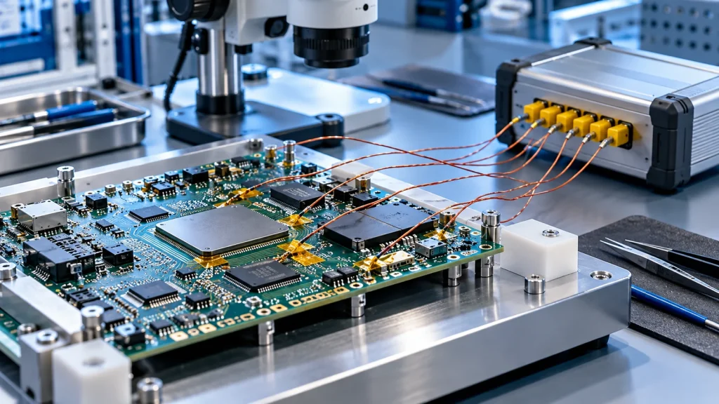
Attach thermocouples using a method appropriate to the measurement site and validate that attachment. Wire routing and attachment can change the measurement or disturb small components. KIC’s published RIT study illustrates that attachment method can affect profiling results and component interaction on densely populated boards; its findings should not be generalized to every assembly or attachment product. [2]
Profile the final masking and pallet arrangement. If mask size, material thickness, tooling or component arrangement changes substantially, review whether the original thermal evidence still applies.
Go beyond visual cleanliness when the risk requires it
Microscopy can identify fragments, staining and visible transfer. It cannot prove the absence of ionic or other transferable contamination. Use analytical testing when it answers a defined failure mechanism, and add surface-insulation-resistance testing on suitable process-representative coupons where electrical reliability requires it.
A bulk ionic extraction result alone should not be treated as proof of long-term electrical reliability. IPC’s guidance distinguishes process monitoring from qualification and discusses SIR-based evaluation. Select methods and acceptance criteria against the applicable customer requirements and agreed standard editions. [5, 6]
Where the mask is removed before service, dielectric strength of the temporary film is usually not the acceptance criterion for the final assembly. If it must provide electrical separation during processing, define voltage, geometry, moisture and exposure conditions explicitly. If the material remains in service, treat it as a permanent insulation design requiring a separate qualification.
Include the uncomfortable corners of the process window
Evaluate the allowed maximum heat exposure and pass count, realistic removal delays, application dwell variation, cleaning sequence, and relevant storage age. Do not intentionally exceed component or assembly limits just to challenge the tape. Distinguish a controlled robustness trial from approved production conditions.
Release only the tested construction and documented operating window. Changes to backing, adhesive, coat weight, liner, source or converting process should trigger a documented change review and proportionate requalification.
8. A practical engineering selection workflow
- Define the function. Identify the feature to protect, why protection is required and when the mask will be removed.
- Classify the exposure. Separate hot air, radiation, local rework and direct molten-solder contact; capture the complete sequence.
- Define interfaces. Record PCB finish, solder mask, topography, flux, cleaning and later coating or bonding.
- Shortlist complete constructions. Review grade-specific documents and eliminate unsupported exposure claims.
- Design the part and presentation. Establish coverage, tolerances, removal access, liner format and placement method.
- Screen representative samples. Check movement, edge integrity and removal before committing to production tooling.
- Qualify the full process. Use the agreed thermal, cleanliness and functional acceptance plan across representative production variation.
- Approve and control. Freeze the construction, drawing revision, work instruction, incoming checks and change-notification requirements.
For roll widths, die-cut presentation or combined conversion steps, use HighTemp Material’s precision converting services as a starting point for a feasibility discussion. Capability and tolerance commitments should be confirmed against the particular construction and drawing.
Compare total applied cost: material, conversion, placement, removal, inspection, cleaning, rejected assemblies and rework. Lower roll price can be offset by slower application or unstable demasking. Run a timed pilot before assuming an economic benefit.
9. RFQ checklist: information that makes quotations useful
| RFQ item | What to provide |
|---|---|
| Function and application | Protected feature, assembly type, temporary or permanent use |
| Process | Reflow, wave, selective soldering or rework; complete operation sequence |
| Thermal evidence | Actual measured profile, peak, dwell, ramps, pass count and atmosphere |
| Solder contact | Direct contact or indirect exposure, contact side, duration and tooling |
| Substrate | PCB finish, solder-mask system, flex/rigid construction and surface condition |
| Material preference | Preferred backing and adhesive; incumbent grade if shareable; restrictions |
| Electrical requirements | Process isolation needs or post-removal functional and cleanliness criteria |
| Geometry | Backing and total thickness, width, part dimensions, drawing and tolerances |
| Presentation | Roll, sheet or die-cut; liner, tab, orientation, core and packaging requirements |
| Chemicals and downstream steps | Flux identity, cleaner, wash/dry sequence, coating, bonding or contact requirements |
| Validation | Required methods, standard editions, acceptance limits and sample plan |
| Documentation | TDS revision, traceability, CoC/CoA where required, relevant declarations |
| Commercial details | Trial quantity, annual demand, order quantity, destination and required date |
If regulatory declarations are required, request documents for the exact supplied construction. RoHS/REACH documentation is not proof of thermal suitability. Do not require or claim UL recognition generically: identify the precise end-use requirement and verify any relevant file, product designation and scope independently.
10. Frequently asked questions
What is the best masking tape for reflow soldering?
There is no universal grade. A qualified polyimide tape is a practical candidate for demanding profiles, but the best choice depends on the actual surface, adhesive, exposure, pass count and removal requirements. Approve the construction only after representative testing.
Can PET masking film replace polyimide tape in lead-free reflow?
Only where the exact PET construction passes the actual process and downstream acceptance plan. A PET backing designation or qualification in another heated process is insufficient. If profile data are unavailable, do not assume equivalence.
Can the same tape be used for reflow and wave soldering?
Possibly, if both exposures are supported and validated. Hot-air survival does not demonstrate resistance to direct molten-solder contact, flux penetration or edge leakage. Test each relevant operation and the combined sequence.
Is solder masking tape a thermal barrier for sensitive components?
A thin film mask should not be assumed to keep a component below its temperature limit. Determine the component’s actual temperature and evaluate a dedicated shield or process change if required. Also check the effect on nearby joint formation.
Does silicone adhesive always leave contamination?
No universal conclusion follows from the adhesive family. Transfer and downstream compatibility depend on formulation, substrate and process. If the assembly is silicone-restricted, request a construction-specific declaration and test the actual downstream operation.
How should clean removal be specified?
Define the removal temperature, delay, angle and rate; identify the surface and inspection method; and set limits for residue, staining, tearing and substrate damage. Add analytical or functional tests when visual inspection does not address the reliability risk.
Is a high dielectric strength necessary for temporary solder masking?
Only when electrical separation is part of the masking function. If the mask is removed before service, final assembly cleanliness and function may be more relevant. A tape dielectric-strength value is not an assembly working-voltage rating.
Can a solder mask be reused?
Do not assume that a single-use adhesive tape or peelable mask is reusable. Heating, contamination and removal can alter it. Reusable pallets and shields need defined inspection, maintenance and retirement criteria, supported by process validation.
Are die-cut masks better than hand-cut strips?
Die-cutting can improve geometry and handling consistency for repeat parts. It does not correct an unsuitable material or process. Validate registration, liner release, removal tabs, operator handling and total applied cost.
What documents should purchasing request before approving a substitute?
Request the exact construction identity, current TDS, traceability, relevant declarations, drawing, test conditions and documented acceptance evidence. Define supplier change notification. Similar color, polymer name or nominal thickness is not evidence of interchangeability.
Discuss your solder-masking requirement with HighTemp Material
Selecting a material is easier when the thermal profile and protected feature are reviewed together. Send HighTemp Material your RFQ with the material preference, application, measured temperature profile, electrical requirements, thickness, dimensions, drawing, required test standards and expected purchase quantity.
Include direct solder contact, flux and cleaning details, pass count, removal conditions and any silicone restrictions. Ask for the candidate construction’s available documentation and an evaluation sample plan before production approval. Material availability, converting feasibility and performance commitments must be confirmed for the proposed grade and application.
Technical references and scope
The guidance in this article is a selection and validation framework, not an HTM product datasheet or a claim of tested performance. No HTM temperature limit, certification or verified test result is established here. External product data apply only to the identified external construction.
- 3M Polyimide Film Tape 5413 technical data, retrieved document dated July 2026. External construction example; typical values are not HTM specifications.
- KIC: Thermocouple Tactics—A Comparative Study of Attachment Methods. Evidence of measurement-method sensitivity under the study’s conditions.
- ASTM D3330/D3330M—Peel Adhesion of Pressure-Sensitive Tape. Method scope; obtain the agreed edition before testing.
- ASTM D3652/D3652M—Thickness of Pressure-Sensitive Tapes. Method reference; confirm the required edition.
- IPC: Changes to cleaning and residue requirements in J-STD-001H. Historical explanation of the shift away from a universal ROSE qualification limit; not a claim that revision H is the latest applicable edition.
- IPC-9203 contents and scope. Process characterization and electrical reliability context; select applicable methods with the customer.