
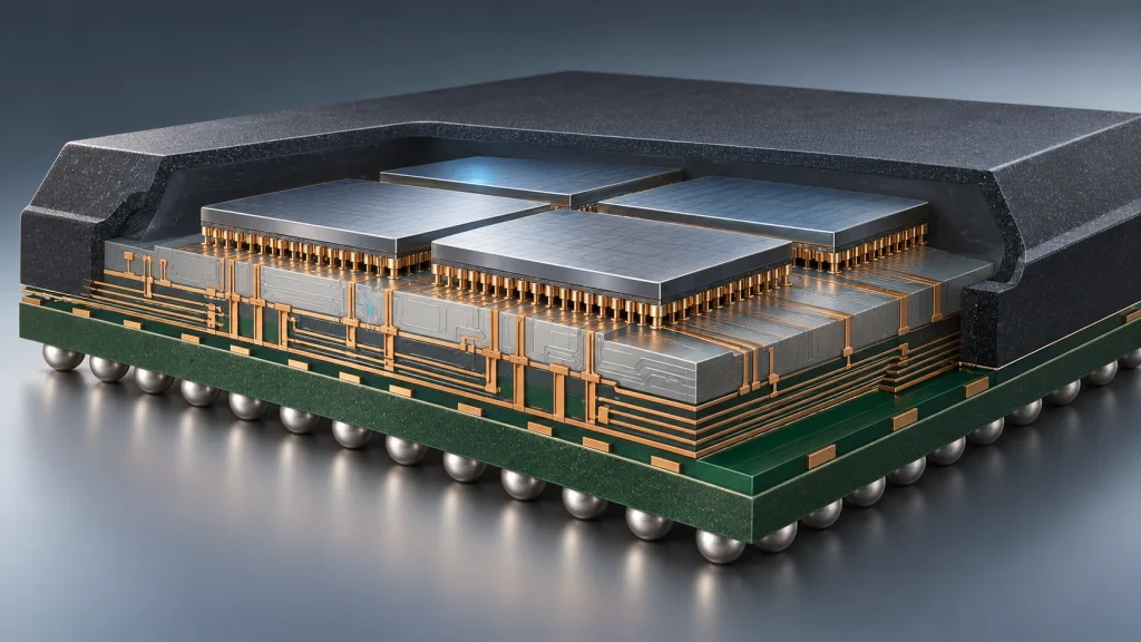
Advanced packaging combines multiple dies, interposers, redistribution layers and fine-pitch interconnections in increasingly compact structures. As package density rises, materials must perform more than a single insulating or protective function.
A dielectric may need to support fine feature formation and withstand repeated thermal cycles. An encapsulant must flow into narrow structures while controlling stress and warpage. A process-support film or converted PI component must remain clean, dimensionally stable and traceable.
These materials cannot be selected as interchangeable “high-temperature plastics.”
Why the Materials Discussion Is Accelerating
Several October 2026 announcements illustrate the direction of the market.
Sumitomo Bakelite announced additional capacity in Suzhou and Singapore for mold underfill and compression-molding granule products used in advanced semiconductor packaging. Fujifilm is highlighting its ZEMATES photosensitive insulating materials at SEMICON West in the United States. GlobalFoundries and TSMC also announced a multi-year arrangement to establish US-based silicon-interposer supply for CoWoS packaging.
Together, these developments indicate growing investment in advanced packaging capacity, regional supply resilience and specialized material systems. They do not mean that every PI film, adhesive or converted insulation component is semiconductor-grade.
Four Material Functions Buyers Must Distinguish
1. Photosensitive polyimide and PBO dielectrics
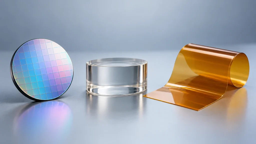
Photosensitive PI and polybenzoxazole materials are used to create insulating or protective layers through semiconductor lithography processes.
Depending on the formulation and process, their functions may include:
- Redistribution-layer dielectric
- Passivation or protective coating
- Stress-buffer layer
- Insulation between conductive features
These materials are engineered for coating or film processing, exposure, development, cure and integration with metals and other wafer-level materials.
A conventional industrial PI film is not a direct substitute for a photosensitive dielectric.
2. Mold underfill and encapsulation materials
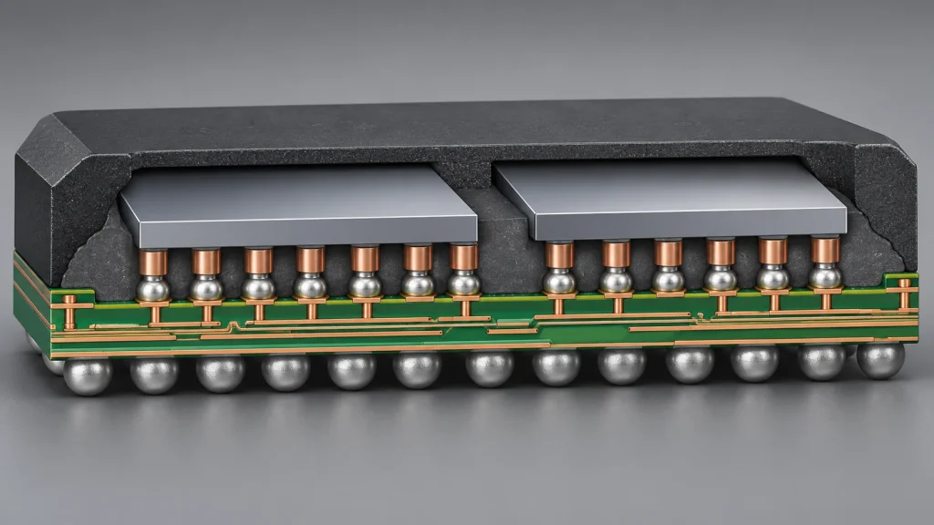
Mold underfill integrates encapsulation and underfill functions in a molding process. Its performance depends on a controlled balance among flow, filler characteristics, cure behavior, adhesion and thermal-mechanical properties.
Important selection factors may include:
- Ability to fill fine gaps
- Cure profile
- Glass-transition behavior
- Coefficient of thermal expansion
- Modulus
- Moisture absorption
- Adhesion to die, substrate and other interfaces
- Warpage contribution
- Ionic cleanliness
- Reliability after thermal cycling and moisture exposure
These are typically highly formulated resin systems. They should not be confused with PI insulation films or silicone sealing materials.
3. Temporary process-support and protection materials
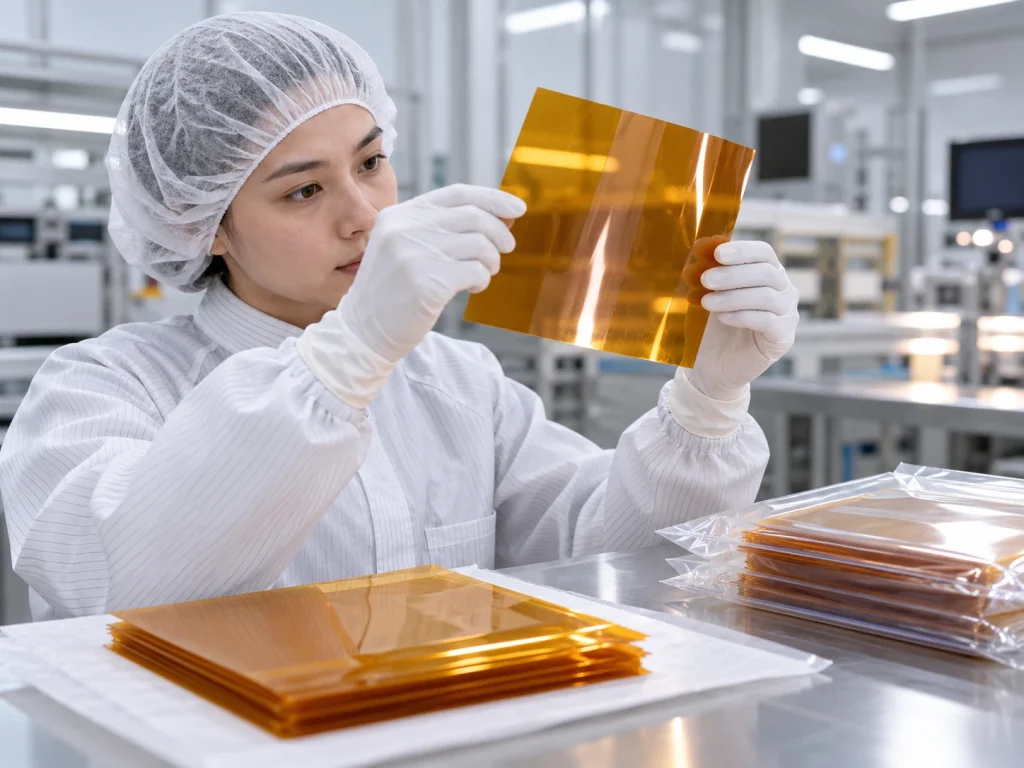
Manufacturing and assembly may require temporary masking, release, cushioning, handling or surface-protection materials.
Here, a PI, fluoropolymer or adhesive-backed film may be selected for:
- Short-duration temperature exposure
- Dimensional stability
- Clean removal
- Chemical resistance
- Controlled adhesion
- Low residue
- Die-cut geometry
Qualification must address the complete construction, including film, adhesive, liner and conversion process.
4. Permanent converted insulation components
Some electronic assemblies use permanent PI films, pads or barriers outside the wafer-level dielectric stack. Their suitability depends on the actual voltage, temperature, geometry, cleanliness and attachment method.
A datasheet value for base PI film does not automatically establish the dielectric performance of a small die-cut component with edges, holes, adhesive and possible contamination.
Polyimide Selection: Form Matters
The term “polyimide” can refer to several commercially distinct forms:
- Non-photosensitive liquid precursor
- Photosensitive liquid PI
- Photosensitive PI film
- Fully cured free-standing PI film
- Adhesive-coated PI film
- FEP-laminated PI film
- Converted PI pad, spacer or barrier
Each form belongs to a different manufacturing step.
A buyer should specify whether the requirement concerns wafer processing, substrate-level redistribution, temporary assembly protection or a permanent mechanical/electrical component.
PFAS-Free Claims Require Precise Interpretation
Fujifilm has previously described PFAS-free innovation across its ZEMATES PI portfolio. For buyers, such a statement should trigger a documentation review, not an assumption.
Questions should include:
- Which substances are included in the supplier’s PFAS definition?
- Does the statement cover intentionally added substances, analytical non-detection or both?
- What test method and detection limits are used?
- Does it apply to every product code and manufacturing location?
- Is the statement designed for a specific regulation or customer standard?
- How will formulation changes be communicated?
“PFAS-free” is not automatically equivalent to compliance with every current or future US state law, EU restriction proposal or customer restricted-substance list.
Key Qualification Parameters
Thermal-mechanical compatibility
Differences in thermal expansion can generate stress, delamination and warpage. Selection should consider the entire material stack rather than one isolated CTE value.
Relevant inputs may include:
- Cure temperature
- Operating temperature range
- Thermal-cycle profile
- Package geometry
- Substrate and interposer materials
- Modulus over temperature
- Glass-transition behavior
- Moisture condition
Dielectric performance
For permanent insulation, review dielectric strength, dielectric constant, dissipation factor and insulation resistance where applicable.
Test frequency, thickness, humidity and specimen preparation matter. Values from different methods cannot be compared without context.
Cleanliness and ionic contamination
Semiconductor and high-density electronics processes can be sensitive to particles, extractable ions, silicone transfer, adhesive residue and outgassing.
An RFQ should define the required cleanliness level and test method. “Cleanroom compatible” without a class, packaging specification or contamination limit is too vague.
Adhesion and interface reliability
Adhesion must be evaluated against the actual copper, passivation, molding compound, substrate or other surface. Surface treatment, moisture, cure and thermal cycling can substantially change the interface.
Process window
A material that performs well under one laboratory condition may be unsuitable for production if its workable temperature, pressure, time or storage window is too narrow.
Buyers should request:
- Recommended process conditions
- Permitted operating range
- Shelf life and storage temperature
- Thawing or conditioning procedure
- Working life after opening
- Rework constraints
- Lot-release criteria
Traceability and change control
Regional supply expansion can improve availability, but it also makes manufacturing-site equivalence important.
Confirm:
- Manufacturing location
- Qualified alternate site
- Raw-material traceability
- Certificate of analysis content
- Lot numbering
- Notification period for formulation, process or site changes
- Retention-sample policy
- Business-continuity plan
Regionalization and US Supply Chains
The announced plan to establish US silicon-interposer supply is strategically important for advanced packaging. From a materials-procurement perspective, regionalization may increase attention to:
- Domestic or regional continuity
- Export-control screening
- Country-of-origin documentation
- Lead-time resilience
- Authorized distribution
- Local technical support
- Auditable change management
Suppliers outside the United States can still compete, but claims must be precise. Stable documentation, controlled packaging and responsive engineering communication are often more credible than broad statements such as “semiconductor grade.”
RFQ Checklist

An advanced-packaging-related RFQ should identify:
- Material function
- Process step
- Substrate and contact surfaces
- Film or coating thickness
- Critical dimensions and tolerances
- Thermal profile
- Required dielectric properties
- CTE, modulus or warpage constraints
- Moisture and chemical exposure
- Particle, ionic and outgassing limits
- Adhesion or release requirements
- Storage and shelf-life expectations
- Packaging and cleanroom requirements
- Required compliance documents
- Sample and qualification quantity
- Forecast volume
- Change-notification expectations
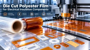
If the requested product is a converted PI film part, include the drawing, adhesive construction, liner, edge-quality requirement and packaging method.
What HighTemp Material Can and Cannot Claim
HighTemp Material offers PI-based films and precision-converted insulation components for relevant industrial and electronic applications. These capabilities can support discussions involving dimensional conversion, adhesive lamination and high-temperature insulation.
They should not be represented as equivalent to photosensitive wafer-level PI, PBO dielectric or mold underfill unless the exact product has been designed, documented and qualified for that process.
The correct starting point is the function—not simply the polymer name.
Conclusion
Advanced packaging growth is creating demand across several distinct material categories: lithographically processed dielectrics, encapsulation compounds, temporary process materials and permanent converted insulation parts.
Successful selection begins by separating these functions and translating package requirements into measurable material, process, cleanliness and traceability criteria.
For a PI film or custom converted insulation inquiry, send HighTemp Material the application step, drawing, thermal exposure, electrical requirement, adhesive construction and cleanliness expectations. The proposed material and documentation scope should then be reviewed against the specific use case.
FAQ
Is ordinary PI film the same as photosensitive PI?
No. Photosensitive PI is formulated for coating or film-based lithographic processing. Fully cured industrial PI film is a separate material form.
Is mold underfill a type of PI?
Typically no. Mold underfill is generally a formulated encapsulation resin system with fillers and cure chemistry designed for molding and gap filling.
What does “semiconductor grade” mean?
The phrase has no useful value without measurable requirements such as particles, ionic contamination, outgassing, traceability, packaging and validated process compatibility.
Can UL recognition qualify a material for wafer-level packaging?
No. UL recognition may address defined safety properties, but it does not establish lithography, contamination, adhesion or semiconductor-process suitability.
What information is needed for a custom PI die-cut RFQ?
Provide the drawing, thickness, adhesive or laminate construction, temperature profile, electrical requirement, cleanliness limits, tolerances, packaging and forecast volume.